




In brief
TOPPAN Inc. says it will install a pilot line at its Ishikawa Plant in Nomi, Japan, to support research and development in advanced semiconductor packaging. The company aims to begin operating the line in July 2026. Work will cover components including large-glass-substrate interposers, glass cores and organic redistribution layer (RDL) interposers. TOPPAN says an organic RDL interposer project was selected for a NEDO-solicited subsidy program and will focus on submicron interconnect fabrication technologies. The company will conduct related development with five academic and research institutions. It also plans to use customer relationships to identify technology needs and development goals, while working with university partners on talent development and recruitment.
Key takeaways
- TOPPAN plans to commission an advanced semiconductor packaging R&D pilot line at its Ishikawa Plant in July 2026.
- The facility will support research on glass cores, glass interposers and organic RDL interposers.
- A NEDO-selected project will develop submicron interconnect fabrication technologies for organic RDL interposers.
- TOPPAN will collaborate with five universities and research institutions on development work.
Driving R&D of glass components for scaling of semiconductor packaging substrates
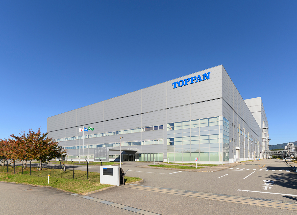
Tokyo, Japan, December 16, 2025 -- TOPPAN Inc. (TOPPAN), a TOPPAN Group company and wholly owned subsidiary of TOPPAN Holdings Inc. (TYO: 7911), will install a pilot line to conduct research and development of advanced semiconductor packaging at the Ishikawa Plant (Nomi, Ishikawa Prefecture, Japan) acquired in 2023, aiming to commission the line in July 2026.
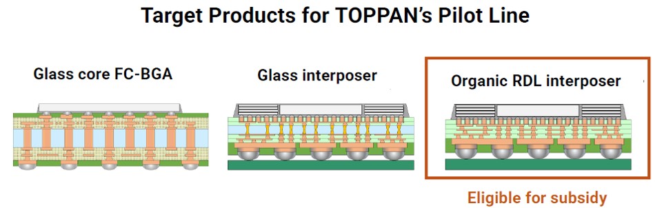
Organic redistribution layer (RDL) interposer development to be conducted on the pilot line has been selected for the Research and Development Project of the Enhanced Infrastructures for Post-5G Information and Communication Systems / Development of Manufacturing Technologies for Advanced Semiconductors (subsidy), for which the New Energy and Industrial Technology Development Organization (NEDO) solicited applications.
In the area of advanced semiconductors used for applications such as generative AI and autonomous driving, packaging substrates are being scaled up and chiplet structures1 are being adopted to achieve higher densities. Chiplet structures require intermediate substrates called interposers2 to connect chips to packaging substrates. Silicon interposers are currently the predominant type, but due to challenges in scaling up, the industry is looking toward the establishment of interposer technology based on large glass substrates as an alternative to silicon.
Utilizing the new pilot line, TOPPAN will verify technologies for future mass production by pursuing R&D on components required for advanced semiconductor packaging, such as interposers using large glass substates as well as glass cores and organic RDL interposers.
The project selected by NEDO aims to simultaneously achieve low power consumption and high-capacity data transfer by developing submicron interconnect fabrication technologies for organic RDL interposers. TOPPAN will advance the development of technologies and materials in collaboration with Osaka Metropolitan University, Toyama Prefectural University, Shinshu University, the Institute of Science Tokyo, and the National Institute of Advanced Industrial Science and Technology.
Future Activities
In addition to R&D, TOPPAN intends to leverage relationships with its long-standing customers to identify advanced technology needs and clarify development targets to increase the speed of manufacturing technology development for glass cores, glass interposers, and organic RDL interposers. Through these efforts, TOPPAN aims to simultaneously achieve high-capacity data transmission and low power consumption. In collaboration with the universities it is working with on joint research, TOPPAN will also advance efforts to develop and recruit talent capable of driving the R&D and related initiatives.
Related Links
NEDO:
About the implementation framework for the Research and Development Project of the Enhanced Infrastructures for Post-5G Information and Communication Systems / Development of Manufacturing Technologies for Advanced Semiconductors (subsidy)
https://www.nedo.go.jp/koubo/IT3_100363.html
(In Japanese)
Ministry of Economy, Trade and Industry:
Notice of business operators selected for the Research and Development Project of the Enhanced Infrastructures for Post-5G Information and Communication Systems (December 3, 2025)
https://www.meti.go.jp/policy/mono_info_service/joho/post5g/20251203.html
(In Japanese)
1. Chiplet: A technology for providing large-scale circuits in a single package composed of multiple small individual chips.
2. Interposer: An intermediate substrate that electrically connects front and rear circuits with through-mold vias.
About the TOPPAN Group
Established in Tokyo in 1900, the TOPPAN Group is a leading and diversified global provider committed to delivering sustainable, integrated solutions in fields including printing, communications, security, packaging, décor materials, electronics, and digital transformation. The TOPPAN Group’s global team of more than 50,000 employees offers optimal solutions enabled by industry-leading expertise and technologies to address the diverse challenges of every business sector and society and contribute to the achievement of shared sustainability goals.
https://www.holdings.toppan.com/en/
https://www.linkedin.com/company/toppan/
If you detect any issues, problems, or errors in this press release content, kindly contact [email protected] to notify us (it is important to note that this email is the authorized channel for such matters, sending multiple emails to multiple addresses does not necessarily help expedite your request). We will respond and rectify the situation in the next 8 hours.
Questions around this news
What will TOPPAN research on the Ishikawa pilot line?
The line is intended for research and development of technologies and materials for advanced semiconductor packaging. Work will include interposers made with large glass substrates, glass cores, and organic redistribution layer (RDL) interposers. TOPPAN says it will use the line to verify technologies that could support future mass production.
When is TOPPAN's Ishikawa pilot line expected to begin operating?
TOPPAN aims to commission the pilot line in July 2026. It will be located at the Ishikawa Plant in Nomi, Ishikawa Prefecture, Japan, a site the company acquired in 2023. The release describes the facility as a research and development line, rather than announcing commercial production there.
Why is the semiconductor industry exploring glass interposers?
The release says silicon interposers are currently the predominant type, but scaling them up presents challenges. The industry is therefore looking at large glass substrates as an alternative basis for interposer technology. TOPPAN plans to research glass interposers and glass cores as part of its broader advanced-packaging work.
What is an organic RDL interposer designed to do?
An organic RDL interposer uses redistribution layers—conductive pathways arranged to route electrical connections between components—to connect chips within an advanced package. The project described in the release will develop submicron interconnect fabrication technologies for these interposers, with the stated aim of supporting both low power consumption and high-capacity data transfer.
Earlier from the TOPPAN Group
- TOPPAN Group Launches Business Supporting Sales of Japanese Anime and Manga Merchandise in UK
- TOPPAN Group Launches Business Supporting Sales of Japanese Anime and Manga Merchandise in UK
- TOPPAN Group Acquires Italian High-performance BOPP Film Company
- TOPPAN Holdings Named to Dow Jones Sustainability World Index for Successive Years
- TOPPAN Holdings Acquires Sonoco’s TFP Business
