




Purchasing land and plant at JOLED Nomi Site as a new base
Tokyo, December 5, 2023 -- TOPPAN Inc. (TOPPAN), a TOPPAN Group company and wholly owned subsidiary of TOPPAN Holdings Inc. (TYO: 7911), has announced that on November 28 it entered into a sale and purchase agreement with OLED developer and manufacturer JOLED Inc. (JOLED) for the land and buildings at the JOLED Nomi Site in Nomi, Ishikawa Prefecture, Japan.TOPPAN plans to use the site to develop next-generation technology and construct a mass production line for Flip Chip Ball Grid Arrays (FC-BGAs) that meet demand for high-speed transmission and chiplet1 use. FC-BGAs are high-density semiconductor packages for which significant growth is anticipated due to increased demand centered on use for data centers and generative AI. TOPPAN expects to launch the new line in 2027 or thereafter and is also considering the production of its existing electronics products at the Nomi Site.
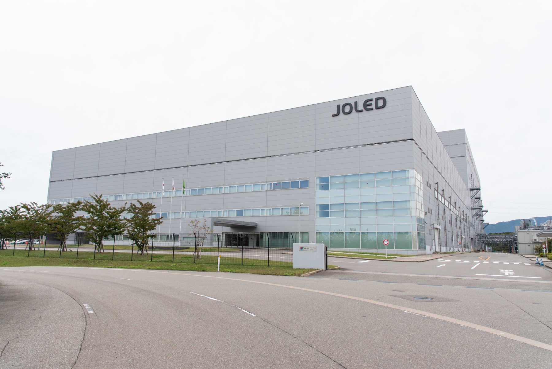 The Nomi Site in Japan’s Ishikawa Prefecture
Background and objectives
With society’s digitalization progressing at pace, the volume of data traffic is increasing every year. This is focusing attention on 2.xD packages2 and other next-generation semiconductor packages that respond to needs for high-speed, large-volume transmission.
TOPPAN is currently expanding FC-BGA production capacity at its Niigata Plant in Japan, but room for future expansion at the plant is limited in the face of fierce demand. The company has therefore been considering how to secure a new production base and identified the JOLED Nomi Site as a location that meets the requirements for next-generation semiconductor package manufacturing processes.
In brief
TOPPAN Inc. says it has agreed to acquire the land and buildings at JOLED’s Nomi Site in Ishikawa Prefecture, Japan, for use as a new semiconductor packaging base. The company plans to develop next-generation technologies there and build a mass production line for Flip Chip Ball Grid Arrays (FC-BGAs), packages intended to support high-speed transmission and chiplet applications. TOPPAN expects the line to begin operating in 2027 or later and is considering making existing electronics products at the site as well. The company says its current FC-BGA capacity expansion at the Niigata Plant faces limited room for further growth. It plans to use digital twin, factory automation and AI technologies at Nomi to support the facility’s launch and production efficiency.
Key takeaways
- TOPPAN agreed to buy the land and buildings at JOLED’s Nomi Site.
- The site is intended for FC-BGA technology development and a mass production line.
- TOPPAN expects the line to launch in 2027 or thereafter.
- The company is also considering making existing electronics products at the location.
Overview
・Assets acquired: Land and buildings of the JOLED Nomi Site
・Location: Nomi, Ishikawa Prefecture, Japan
・Site area: 99,612.14 m2
・Building area: 100,683.40 m2
・Date of sale and purchase agreement: November 28, 2023
Future
TOPPAN will push forward with development of next-generation semiconductor package technologies and the construction of a mass production line expected to go live in 2027 or thereafter. TOPPAN will use digital twin,3 factory automation, and AI technologies to target the smooth launch of a state-of-the-art facility that reduces manpower needs and drives high production efficiency.
1. Chiplet: A technology for providing large-scale circuits in a single package composed of multiple small individual chips.
2. 2.xD package: A semiconductor package featuring a fine wiring substrate called an interposer between the chip and the resin substrate.
3. Digital twin: A technology for digitally replicating the objects and data of a real space.
About the TOPPAN Group
Established in Tokyo in 1900, the TOPPAN Group is a leading and diversified global provider committed to delivering sustainable, integrated solutions in fields including printing, communications, security, packaging, décor materials, electronics, and digital transformation. The TOPPAN Group’s global team of more than 50,000 employees offers optimal solutions enabled by industry-leading expertise and technologies to address the diverse challenges of every business sector and society and contribute to the achievement of shared sustainability goals.
https://www.holdings.toppan.com/en/
https://www.linkedin.com/company/toppan/
If you detect any issues, problems, or errors in this press release content, kindly contact [email protected] to notify us (it is important to note that this email is the authorized channel for such matters, sending multiple emails to multiple addresses does not necessarily help expedite your request). We will respond and rectify the situation in the next 8 hours.
Questions around this news
What will the new Nomi facility produce?
The site is intended to support development of advanced semiconductor-package technology and a high-volume manufacturing line for Flip Chip Ball Grid Arrays (FC-BGAs). The packages are designed to serve applications requiring fast data movement and chiplet-based designs. The company is also evaluating whether to make some of its existing electronics products at the site.
Why was the JOLED Nomi Site selected for the project?
The release says the company needs another manufacturing base because space for further expansion at its Niigata Plant is limited, while demand for FC-BGA capacity is strong. It identified the Nomi location as suitable for the processes needed to make next-generation semiconductor packages.
When is the planned production line expected to begin operating?
The company expects the new mass-production line to become operational in 2027 or later. It plans to develop packaging technologies and build the line at the Nomi site, using digital-twin, factory-automation and AI technologies to support an efficient facility with lower staffing requirements.
What is an FC-BGA package, and where is this type of package used?
A Flip Chip Ball Grid Array is a high-density semiconductor package that connects a chip to a circuit board through an array of small solder balls. Such packages support dense electrical connections and are used in demanding computing applications, including data-center systems and products that require high-speed data transmission.
