




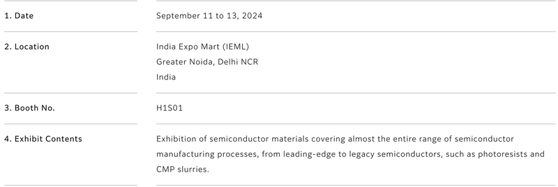
September 3, 2024 -- FUJIFILM Corporation will participate in “SEMICON India 2024”, an international exhibition of semiconductor manufacturing equipment and materials, to be held in New Delhi, India, from September 11 to 13, 2024.
Fujifilm offers semiconductor materials used in wafer processing to post processing in semiconductor manufacturing including photoresists*1, photolithography-related materials, CMP slurries*2, post-CMP cleaners*3, thin-film chemicals*4 and polyimides*5, as well as WAVE CONTROL MOSAIC™*6 which includes color filter materials for image sensors. In addition to its extensive product lineup covering almost the entire range of semiconductor manufacturing processes, from leading-edge to legacy semiconductors, Fujifilm is committed to solving customers' issues by providing one-stop solutions that leverage its global supply structure with 20 locations and advanced R&D capabilities. At the same time, the company is making aggressive capital investments in production facilities globally, and is expanding production capacity and local production of semiconductor materials.
At a glance
- Company
- FUJIFILM Corporation
- Announcement
- Event
- Location
- New Delhi, India
Key figures
- Global supply structure locations
- 20 locations
- India semiconductor-related market forecast
- 64 billion dollars by 2026
- Market size comparison
- about three times the size of 2019
Products and programs
The semiconductor-related market in India is expected to grow to 64 billion dollars by 2026, about three times the size of 2019, due to the government's focus on fostering the semiconductor industry*7.
Through its participation in “SEMICON India”, Fujifilm will accelerate the development and provision of semiconductor materials that meet customer needs and contribute to the development of the semiconductor industry in India by further strengthening its business base in the Indian market.
- * WAVE CONTROL MOSAIC is a registered trademark or trademark of FUJIFILM Corporation.
- *1 Material used to coat wafer substrate when circuit patterns are drawn in the process of semiconductor manufacturing
- *2 A polisher for evenly levelling semiconductor surface, which contains a mixture of wires and insulation films of varying hardness.
- *3 Cleaners used after polishing with CMP slurry to remove particles, minute metal fragments and organic residues while protecting the metal surface
- *4 Materials for forming low-dielectric insulation films
- *5 A material with strong heat resistance and insulation properties, used for forming semiconductors’ protective films and rewiring layer
- *6 General term referring to a group of functional materials for controlling electromagnetic light waves in a broad range of wavelengths, including photosensitive color materials for manufacturing color filters for image sensors such as CMOS sensors, used in digital cameras and smartphones
- *7 According to “Expectations for Experience and Knowledge of Japanese Companies: Exploring the Present State of India's First Semiconductor Manufacturing (4)” by Japan External Trade Organization
Overview of “SEMICON India 2024”
Learn more about “SEMICON India 2024”
Contact
Media Contact
FUJIFILM Holdings Corporation
Coprorate Communications Division,
Public Relations Group
+81-3-6271-2000
Customer Contact
FUJIFILM Corporation
Electronic Materials Business Division
+81-45-534-8824
If you detect any issues, problems, or errors in this press release content, kindly contact [email protected] to notify us (it is important to note that this email is the authorized channel for such matters, sending multiple emails to multiple addresses does not necessarily help expedite your request). We will respond and rectify the situation in the next 8 hours.
In brief
FUJIFILM Corporation says it will take part in SEMICON India 2024, an exhibition of semiconductor manufacturing equipment and materials scheduled for September 11–13 in New Delhi. The company plans to present materials for semiconductor production, including photoresists, CMP slurries, post-CMP cleaners, thin-film chemicals, polyimides and WAVE CONTROL MOSAIC. Fujifilm says its products serve processes ranging from leading-edge to legacy semiconductors, and that it provides customer support through a global supply structure spanning 20 locations and its research and development capabilities. The company also says it is investing in production facilities worldwide to increase capacity and local production. Citing expected growth in India’s semiconductor-related market, Fujifilm says it aims to strengthen its Indian business base and develop materials responsive to customer needs.
Key takeaways
- Fujifilm will participate in SEMICON India 2024 in New Delhi from September 11 to 13.
- The company offers materials for multiple semiconductor manufacturing stages, from wafer processing through post-processing.
- Fujifilm says it is expanding production capacity and local production of semiconductor materials.
- The release cites a forecast that India's semiconductor-related market will reach $64 billion by 2026.
Earlier from FUJIFILM Corporation
- Fujifilm launches “FUJINON HZK14-100mm”- Duvo Portable
- Fujifilm Launches Smartphone Printer “instax mini Link 3™”
- Fujifilm Launches “instax mini Evo™ FUJIFILM 90th Anniversary Special Kit”
- FUJIFILM Holdings President and CEO Teiichi Goto Awarded the Medal of Friendship by the President of Mongolia
- New NURA Health Screening Center Opens in Ulaanbaatar
